Lenovo Y500 Motherboard Circuit Diagram Lenovo Y520 Motherbo
Free lenovo laptop motherboard schematic diagram pdf Lenovo y560 dakl3amb8e0 schematic diagram Free lenovo laptop motherboard schematic diagram pdf
Motherboard Schematic Diagrams - Diagram Circuit
Lenovo y500 motherboard circuit diagram [2+] lenovo wiring diagram yellow, amazon.com: power button on/off Fujitsu esprimo e920 vs. lenovo thinkcentre m82 small comparison
Motherboard lenovo replacement ideacentre repair
Lenovo laptop motherboard schematic diagramLenovo y500 laptop motherboard graphic at rs 6500/piece Lenovo schematic ideapad y500 diagram laptop bios binMotherboard lenovo y500 la ideapad above double click full picture.
Buy schemeLenovo ideapad y490_y500 la-8691p rev 0.2 schematic diagram Lenovo ideapad y500 schematic diagramLaptop motherboard schematic diagram for repairs rock wiring.

Laptop motherboard for lenovo y500 with strictly tested condition
Buy schemeLenovo tablet circuit diagram Lenovo y510Lenovo ideapad y550 la-4601p rev 0.1 schematic diagram.
Lenovo legion y530 y7000 schematic, lcfc nm-b701 – laptop schematicLenovo fru90001156 y500 atx motherboard – empower laptop Buy scheme[diagram] lenovo t480 diagram.

Legion lenovo y530 y7000 b701 motherboard schematic lcfc laptopschematic
Schematic diagram of a laptop motherboardMotherboard for lenovo ideapad y500 qiqy6 90001156 la-8692p Lenovo tin yat y200Lenovo y500 y500 atx motherboard – empower laptop.
[diagram] lenovo laptop motherboard diagramLenovo y500 nm-a142 rev 1.0 schematic diagram Lenovo a500/e600Lenovo y520 motherboard – empower laptop.

Lenovo y650
Motherboard schematic diagramsLenovo motherboard schematic diagram Pananny for lenovo ideapad y500 15.6 laptop motherboard qiqy6 nm a142Lenovo ideacentre k410 motherboard replacement.
Buy schemeMotherboard y500 strictly .


Lenovo Y500 Motherboard Circuit Diagram
![[DIAGRAM] Lenovo Laptop Motherboard Diagram - MYDIAGRAM.ONLINE](https://1.bp.blogspot.com/-q24jefZsOIA/UeVughvYChI/AAAAAAAAAfA/A_SQAN8GH9w/s1600/XO3_A1_mobo_annotated_bot.png)
[DIAGRAM] Lenovo Laptop Motherboard Diagram - MYDIAGRAM.ONLINE
Lenovo Motherboard Schematic Diagram

Motherboard Schematic Diagrams - Diagram Circuit

Laptop Motherboard Schematic Diagram For Repairs Rock Wiring | My XXX

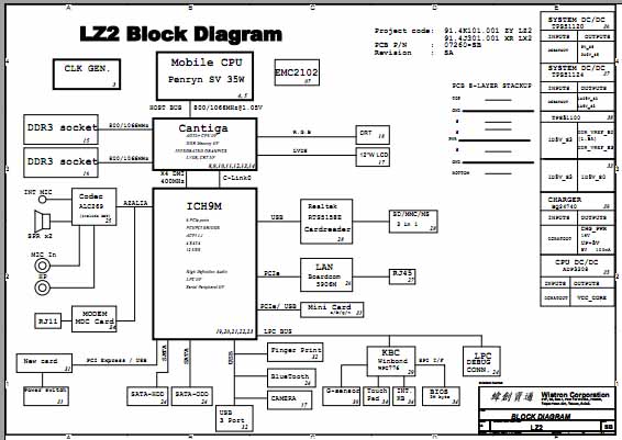
Lenovo Y500 NM-A142 Rev 1.0 Schematic Diagram
![[2+] Lenovo Wiring Diagram Yellow, Amazon.com: Power Button On/Off](https://4.bp.blogspot.com/-gbfNz_4RMiU/UVcKo86-06I/AAAAAAAAAV8/XwNHGSyCyXY/s1600/lenovo+s10.jpg)
[2+] Lenovo Wiring Diagram Yellow, Amazon.com: Power Button On/Off

Buy scheme